Add 3D Models to Symbols
Article published September 16th 2024!
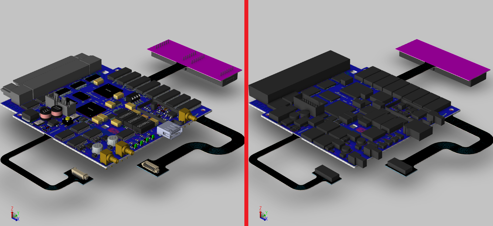
Allegro PCB Editor has always been trying to bridge the gap between electrical engineers and mechanical engineers primarily because how critical it is for these two professions to work cohesively to enable a successful project. When you think of any hardware device, you immediately typically envision the enclosure and casing around it. The mechanical aspects are visible, whether they be the material finish, the mass, or general structure. The internal electrical printed circuit board is hidden inside the mechanical casing but equally important if not more, to ensure proper operation of the device. Understanding the intermingling of the electrical and mechanical aspects, one can understand why the ECAD tools have begun to incorporate some of the features which are traditionally seen only in the MCAD tools. One of which is the ability to provide a 3D rendering of the design to visualize the physical characteristics. Allegro PCB Editor offers a 3D canvas in which the design can be appreciated from several dimensions providing a comprehensive look-and-feel of the final result if it were to be fabricated and assembled with components.
STEP Models
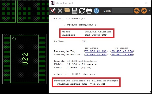
In order for the electrical design to be represented in a 3D format, the components need to have an appropriate model assigned to them. The representation can be as realistic as one wishes or as minimal as required. The bare minimum comprises of the bounding area matching the footprint symbol and a package height value. This is assigned to the DFA_BOUND subclass and can be viewed by identifying the respective shape and clicking "Show Element".
This is sufficient in certain cases such as to allow for mechanical intereference check but by no means something you would present to a public audience. For enhanced visual presentation, more details are preferred and these are often captured in .step model format files. These .step models are often provided by the component vendors and can be imported in the Allegro PCB Editor tool. There are two approaches in utilizing and assigning .step models in the Allegro PCB Editor environment. One can attach the model to the device in the design or attach the model to the symbol drawing. Identifying the symbol and clicking "Show Element" will expose if a .step model has been attached to the symbol drawing. The name of the model along with it's orientation information will be visible in the PKGDEF_STEP properties under the SYMBOL definition or COMPONENT definition.
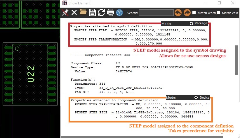
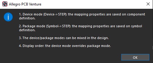
Although it is possible to attach models both to the component in the design and to the symbol drawing, it's worth keeping in mind that the component instance definition (Device Mode) representation will take priority. To showcase the built-in capabilities within Allegro PCB Editor, we will demonstrate both methods of assigning .step models.
Methods for assigning models
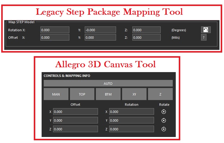
The first step is to procure the .step model of the component of interest. Once that is available, the user has two options available in terms of the tools capable of completing the next steps. The legacy "Step Package Mapping" tool can be used or the newly released "Allegro 3D Canvas" can be used. For demonstration purposes, we will first utilize the legacy Step Package Mapping tool to assign the step model to the symbol drawing and then proceed with assigning another step model to the device in the Allegro 3D Canvas. To reiterate, the order of precedence is shown below. Device Mode (Component Definition) overrides Package Mode (Symbol Mode).
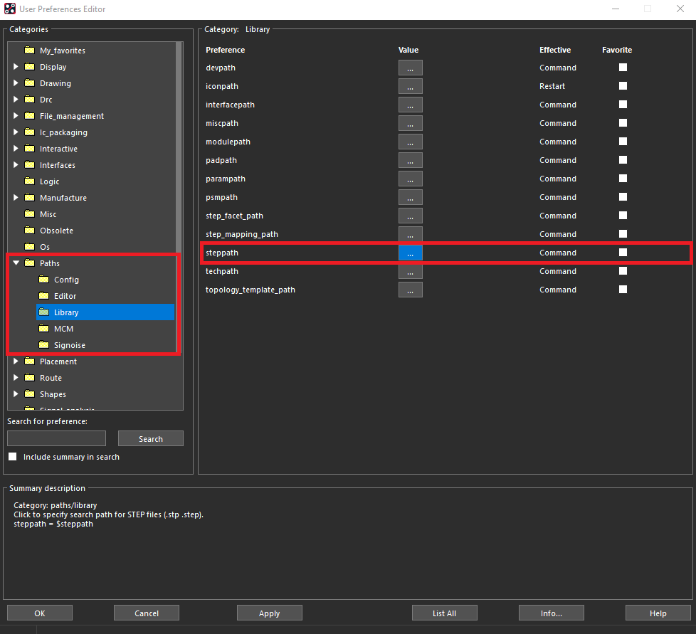
But before either of these tasks can begin, the user needs to ensure the library paths are set appropriately. In order for the .step models to be recognized in the Allegro PCB Editor environment, the respective directories need to be listed appropriately. The default path for the .step models is the STEPPATH variable which points to the Cadence installation at C:/Cadence/*Version*/share/local/pcb/step. Either additional models should be stored in this directory or the appropriate directory should be listed in the STEPPATH environment variable. These settings can be modified from the Setup -> User Preferences window.
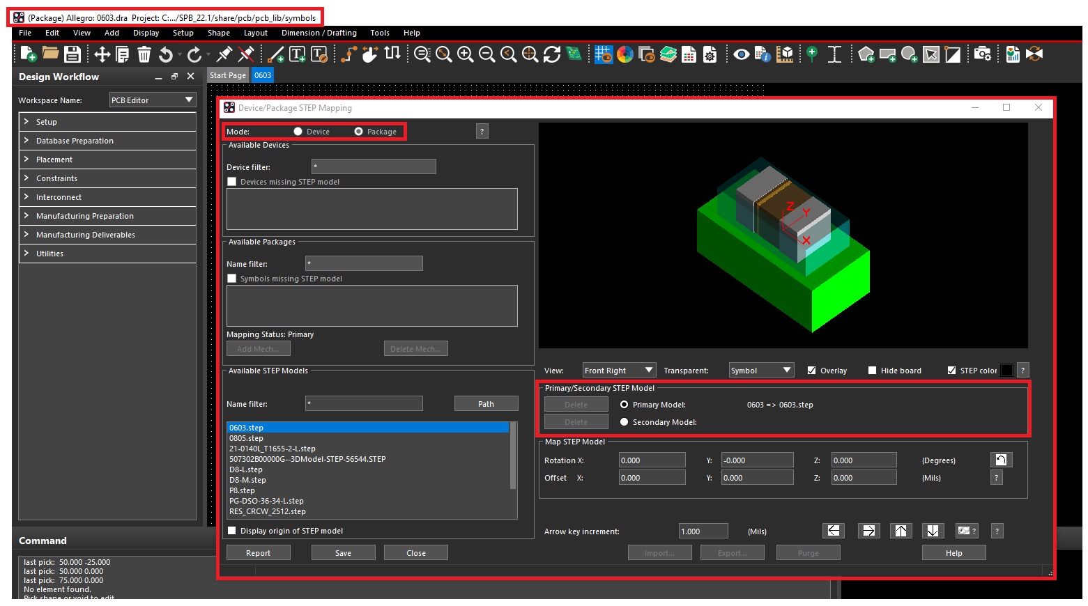
Assign to symbol using the Step Package Mapping tool
The Step Package Mapping Tool can be accessed from the Setup Menu. The Mode radio button should be set to "Package". This will consequently only allow selection of symbols in the Available Packages section. The Available Devices sections will not be selectable. Ideally the mapping process is being completed on the .dra symbol file as this will ensure the step mapping stays fixed permanently to the package. This effectively carries the step model information with the symbol across all designs in which it may be used. Any existing designs leveraging the same footprint can simply do a symbol refresh to update with the latest step model linkage.
Assign to symbol using the Allegro 3D Canvas tool
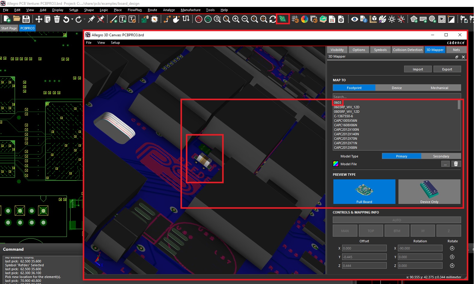
The alternative approach to using the legacy Step Package Mapping tool is the Allegro 3D Canvas tool. The 3D Canvas tool incorporates additional features beyond step model assignment. The 3D rendering of the board design is visible in this canvas and also enables customization of the display characteristics. The key goal of assigning step models and defining their orientation with respect to the footprint drawing are accomplished in the 3D Mapper tab as shown in the snapshot below. Once again, since mapping is done to the Package (labelled footprint) and not the Device, the intention is it will be permanently linked to the symbol drawing. That is of course with the understanding this task is being completed on the .dra file. The example below showcases assignment from a .brd file which will not be a permanent linkage. One can review the footprint symbol details (Show element) directly from the respective .dra file.
Assign to device using the Allegro 3D Canvas
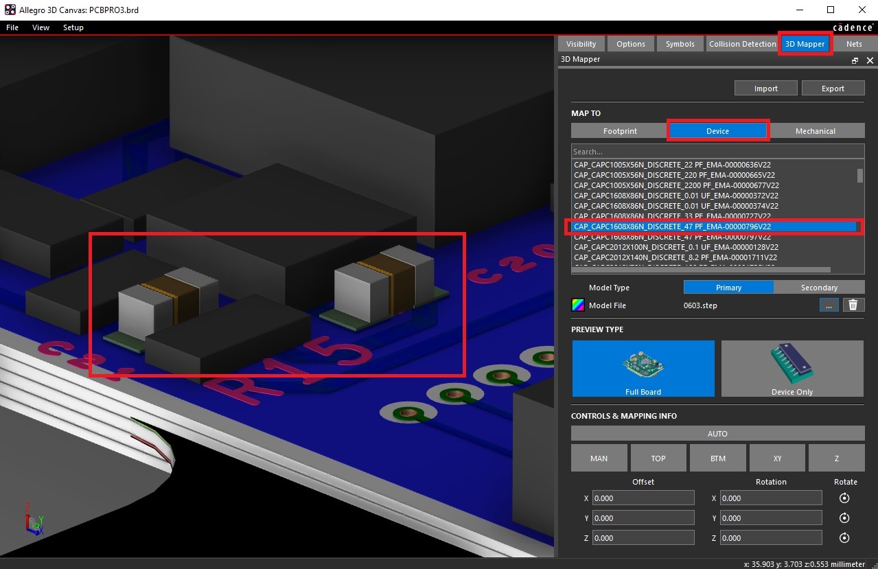
The other approach to attach the step model to the footprint is to link it to the component device. This approach is typically performed from a .brd file and also is a solution best suited to be encapsulated within a particular design. In other words, it is a temporary linkage to the footprint contained to only within the design. This action will not propogate to other designs using the same symbol as it did in the previous method which we discussed. The assignment task can be completed in the legacy Step Package Mapping tool or the newer Allegro 3D Canvas yielding similar results. The 3D Mapper tab in the Allegro 3D Canvas is shown below which showcases similar features as the legacy Step Package Mapping tool but with a more modern and intuitive interface.
Confirm step model orientation
Once the .step model has been sourced for the component of interest, the final step is to begin the mapping process. This task is required to ensure the orientation of the symbol footprint aligns with the 3D model. The x, y, and z coordinate offset along with the rotation parameters need to be adjusted accordingly to ensure a proper alignment. This procedure is needed regardless of whether the legacy step package mapping tool is used or the newer Allegro 3D Canvas tool.
Summary
The task of assigning 3D Step models is very much simplified in Allegro PCB Editor. Two methods exist, one being the legacy step package mapping tool and the other being the 3D Canvas tool. It is critical that the step models be accurate of the component to ensure the proper dimensions are being incorporated in the 3D rendering. This is necessary not only for the visual representation but also in case the printed circuit board is to be enclosed within some mechanical constraints for which interference checks need to be conducted. The proper heights, widths, and lengths are critical to gain confidence in the complete design before releasing for fabrication and tooling.
Component Placement
Careful placement of components is critical to a successful design
Schematic Capture

Creating schematic symbols, drawing the circuit, and generating the netlist
Generate Gerbers


Comments
Add your comments in the section below